
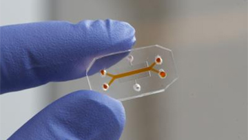
In recent years, microfluidic circuits and systems have been increasingly incorporated into biological instrumentation and used for high-throughput biology experiments. The ability to isolate specific cells or perform PCR in a large-scale format using minimal solution volumes in an instrument with a small footprint are all outcomes of the continued advances in microfluidic technology.
While such microfluidic chips and instruments have expanded in number, the ability to individually customize microfluidic designs or create unique microfluidic-based chips for use in individual labs remains the domain of well-trained chemists and engineers who have access to, and an understanding of, sophisticated manufacturing processes such as soft lithography that are beyond the scope of the traditional biologist. But it soon may be possible for any lab with an interest in creating their own microfluidic designs in-house to construct lab-on-a-chip solutions using readily available building blocks.
In the October issue of the Proceedings of the National Academy of Science, Noah Malmstadt and his colleagues at the University of Southern California in Los Angeles describe their recent work developing a unique “plug-and-play” system that not only makes microfluidic circuit design and construction easier, but also for the first time enables three-dimensional microfluidic architectures.
“The idea came from my PhD student Krisna Bhargava, who has a background in Electrical Engineering. He's used to assembling circuits from a set of standard modular components (resistors, capacitors, diodes, etc.) and found it frustrating that there wasn't a similar design methodology available for microfluidic systems,” recalled Malmstadt.
Taking their cues from the well-established fields of electrical engineering and circuit design, Malmstadt and Bhargava began designing components that could fit together to form complex microfluidic circuits. The researchers decided that all of their microfluidic components would be built to a standard, cubic-geometric size with inlet and outlet elements on the sides to fit widely available tubing.
“There's nothing inherent about the cubic geometry that makes it ‘best’ for this particular approach. In some respects, we chose it because it was the simplest choice and produced circuits in which the connectivity was easy to visualize,” explained Malmstadt. And the cubic geometry did make sense for ease of fabrication since the printing technology they used—stereolithography—is a layer-by-layer process.
The other advantage in adapting the electronic circuit concept to microfluidics was that Malmstadt’s team could now use tools like network analysis that had been developed for classic electronic circuit design to make predictions about fluid flow and mechanics within a microfluidic circuit.
Layer-by-layer fabrication of Malmstadt’s new components also enables the design of 3-D microfluidic configurations that had previously been difficult to achieve. And 3-D architecture means something very important in circuit design: parallelization.
“The way to leverage the advantages of microfluidics for industrial-scale chemical production is to run many devices in parallel, much like how a modern supercomputer works by running many off-the-shelf microprocessors in parallel,” said Malmstadt. Channels arranged in three dimensions rather than two allow researchers greater flexibility and more possibilities in constructing new microfluidic circuit elements.
In the future, Malmstadt hopes to make his modular assembly approach as widely available to researchers and students as possible. “We'd love to develop a community of users. We're thinking of an open-source model where members of the community can share designs for new modules and ideas for connecting them into practical devices.”
Via:biotechniques.com
